Simple Microwave LO using an ADF4350 Module
By Paul McMahon VK3DIP
As appeared in NERG NEWS November 2020
Back
Home
Source Etc.
PC Board Artwork in Sprint Layout Format
Last March during the Corona affected John Moyle Contest I noticed, that my 2.4GHz transverter needed some work. There was obviously some sort of connection between the mains and the case, it still worked fine but touching the metal case gave a bit of a bite. Investigation back home later narrowed it down to an old transformer in the power supply, however as I had originally bought the lot as a going concern at a hamfest I didn’t have a circuit diagram of what did what. So I decided to basically rebuild the whole thing just reusing those bits I had data on. This didn’t seem too hard as the majority of the transverter proper was a couple of kit modules from minikits in South Australia for which the doco was downloadable. One of the modules was the Local Oscillator chain which consisted of a 94MHz crystal oscillator followed by a couple of filter/multiplier (x6 and x4) stages to give the 2256MHz LO (2.4GHz less the 146MHz IF). This has always been a bit off (10kHz at 2.4GHz) and it was the version that didn’t have a heater for the crystal so I thought I would update it a bit and make use of a Analog Devices ADF4350 synthesiser/clock source. These devices are readily available on ebay/aliexpress for around $22 ( depending on current exchange rates) and have the twin advantages of producing output directly at the required 2.256GHz and have the possibility to lock to an external oscillator. There are also ADF4351 versions out there (35MHz to 4.4Ghz, rather than 137.5MHz to 4.4GHz) for slightly more money but this was not worth it in my case. There seems to be two main ADF4350 module versions available examples of which are shown below in Figure 1.
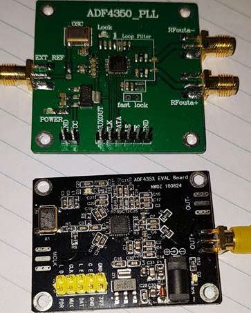
Figure 1- Different ADF4350 boards, top 10MHz onboard, bottom 25MHz.
Apart from the onboard oscillator difference (10MHz vs 25MHz) the 25MHz one is slightly smaller and usually cheaper, yet has more items brought out on the header. In my case I intended to use an external reference oscillator so the onboard one didn’t matter, however for my initial tests it was convenient to use the one with the 10MHz on board so that is what I ended up using, however the other one would have been just as good in the final product, and already has a 3.3V output on the header, so is in fact slightly easier to use.
These boards require something to talk to them to setup frequency etc. I considered briefly using an Arduino to do this as much code is available for this, but it is a bit of overkill as I probably would never want to actually have variable frequencies. Also the ADF4350 requires 3.3V logic levels and while level converters for Arduinos are relatively cheap, it is extra bother. So instead I ended up basing what I did on the work of Ron G7DOE (https://wiki.batc.org.uk/ADF435x_PIC) where he used a small 8 pin PIC instead, running this at 3.3V directly from the regulator on the ADF4350 board.
In Rons version the PIC is a 12F629 or the somewhat more powerful 12F1552, seeing I had a number of 12F629’s from a previous project that is what I went with, however as Ron’s code examples only had the very basic version for the 12F629 I ended up rewriting his code to squeeze a bit more into the 12F629.
To make the code as simple and small as possible the technique used is to work out the register values that need to be programmed into the ADF4350 first and effectively hard code them in the program.
The simplest way to get the register values is to use the free AD ADF435x tool from here: https://www.analog.com/media/en/evaluation-boards-kits/evaluation-software/ADF435x_v4_5_0.zip.
This software is actually intended to be used with the official AD evaluation kit so we only need to use part of it, the register calculation form. (Figure 2)
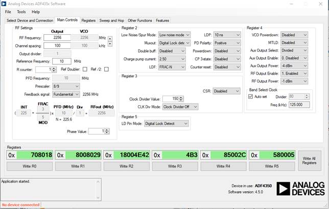
Figure 2- AD ADF435x application.
The items we need to set are of course the output frequency (2256MHz), the reference frequency (10MHz), the Muxout (Digital Lock detect), and the RF output power to whatever level you need. In my case I actually got the register codes for all four output power level possibilities as my code uses the couple of spare pins to select alternatives.
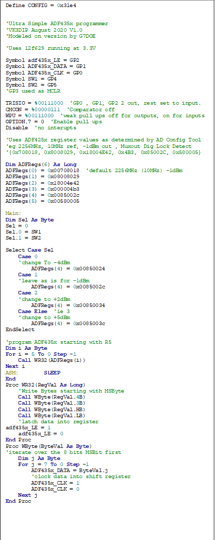
My code (using OshonSoft PIC Basic because I paid for it some years ago and feel I should therefore use it,) is shown below. As you will see it is very simple, basically check the select pins, send the appropriate register values, and stop. I took some pains not to use the same algorithms as in the G7DOE “C” version which in turn came from an Arduino version, ie. no multiply instructions, which are easy to read but which add considerably to the required library code. By doing this I was able to fit this version into the 12F629 which was not possible using G7DOE’s version. My code and the resultant Hex suitable for programming a 12F629 can be got from here:
If you want to set your own frequencies etc. you can get the OshonSoft compiler etc. from here:
https://www.oshonsoft.com/pic.html
 Having
got the code working, I could test it against the board with the 10MHz onboard.
By itself, the ADF4350 can’t deliver the +7dBm out that the MiniKits
transverter module needs for the LO, so I needed some additional gain.
For this I used a SPF5189 MMIC, in my case on one of my own boards, but ebay
etc. have many examples of prebuilt SPF5189 modules. The SPF5189 has a number
of advantages as a MMIC, first of all on ebay at least it is much cheaper than
the PGA103 which it is broadly equivalent too, it can be run from 5V, and has a
P1 (effectively output power while still linear) of about 23dBm ( at 1.92GHz)
which easily should handle the +7dBm requirement, over the frequency
range 50MHz, to 4GHz. I put the board together, connected it up to the ADF4350
board and I could now select, using the selection jumpers on my 12F629 board, a
number of power levels which had a value of about the 7dBm in one of the middle
power levels, I could also go higher if I needed to for a higher drive mixer,
or lower . My version of the SPF5189 board is shown in Figure 3. This version
actually got a little warm over time so I ended up putting a couple of mounting
holes on either side of the MMIC to conduct heat to the case.
Having
got the code working, I could test it against the board with the 10MHz onboard.
By itself, the ADF4350 can’t deliver the +7dBm out that the MiniKits
transverter module needs for the LO, so I needed some additional gain.
For this I used a SPF5189 MMIC, in my case on one of my own boards, but ebay
etc. have many examples of prebuilt SPF5189 modules. The SPF5189 has a number
of advantages as a MMIC, first of all on ebay at least it is much cheaper than
the PGA103 which it is broadly equivalent too, it can be run from 5V, and has a
P1 (effectively output power while still linear) of about 23dBm ( at 1.92GHz)
which easily should handle the +7dBm requirement, over the frequency
range 50MHz, to 4GHz. I put the board together, connected it up to the ADF4350
board and I could now select, using the selection jumpers on my 12F629 board, a
number of power levels which had a value of about the 7dBm in one of the middle
power levels, I could also go higher if I needed to for a higher drive mixer,
or lower . My version of the SPF5189 board is shown in Figure 3. This version
actually got a little warm over time so I ended up putting a couple of mounting
holes on either side of the MMIC to conduct heat to the case.
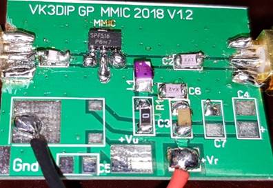
Figure 3- SPF5189 Board.
So all up my final setup is as per Figure 4.
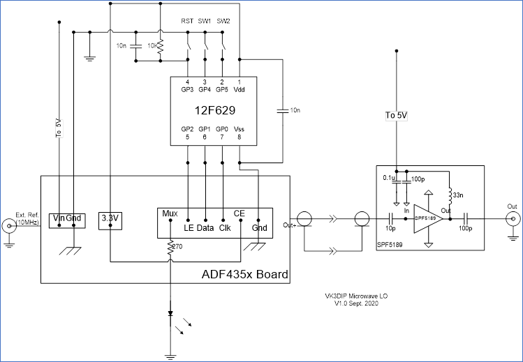
Figure 4 - Overall Schematic
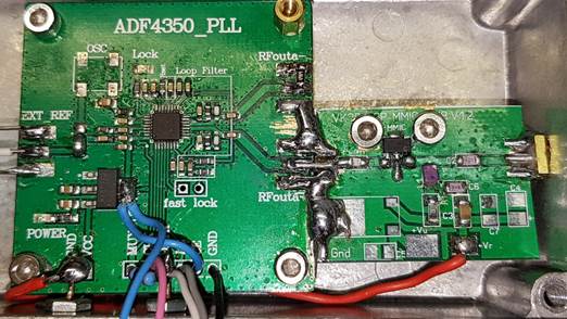
Figure 5 - ADF4350 board and amp
Figure 5 shows the ADF4350 and Amp boards as modified.
On the ADF4350 board:
1. I removed the 10MHz on board oscillator because I didn’t need it, and it may create noise if I left it.
2. Changed the solder jumper to select the external reference. In this case this was just a solder blob, but in the other version it is 0 Ohm links which are both provisioned.
3. Terminated the unused RFouta- with a 49.9 Ohm resistor, two 100 Ohms in parallel would do fine also.
4. Created a 3.3V out by soldering to the tab (ie. equiv. to the centre or out pin) on the onboard regulator.
5. Removed the pin header strip so I could directly solder on the wires, also used the 270Ohm resistor as a jumper from the muxout to a feedthrough for the lock led out.
On the SPF5189 Board:
1. Shortened it a bit, because I initially tried to fit it into a smaller diecast box than the Jaycar HB5062 111x60x30mm one. This will depend on individual circumstances.
2. Drilled a couple of additional mounting holes either side of the SPF5189 to distribute heat to the case via some tapped brass standoffs.
3. Didn’t populate the onboard regulator instead run direct from 5V via a feedthrough.
4. Butt soldered the two boards RF out to in to save connectors etc.
My first shot at the PIC board was on a scrap of protoboard, as in Figure 6, this worked fine and I could have left it at that.
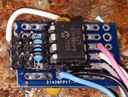
Figure 6 - Initial prototype of PIC 12F629 Board
This was a bit hard to mount in the box, so I did a quick PCB layout and made a dozen or so boards via toner transfer, they are only 1inch square. The result is Figure 7. Figure 8 is the artwork if I ever decide to have it profesionally made.
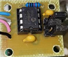
Figure 7 - 12F629 on homemade PCB
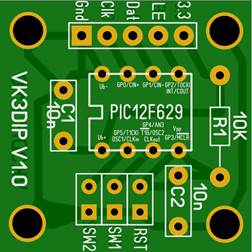
Figure 8 Final PIC PCB 25mmx25mm
The complete assembled LO is shown in Figure 9, the pic board is mounted upside down using one hole and an additional threaded standoff .
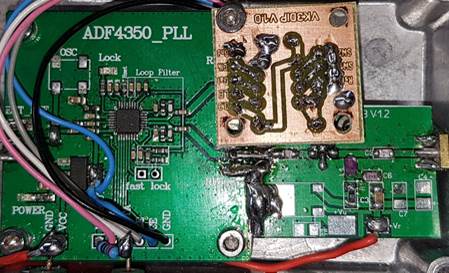
Figure 9 - Installed in Box, note PIC board mounted upside down on standoff over main board.
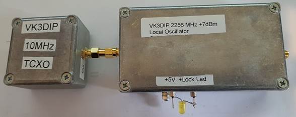
So how does it work? With an external TCXO ( which is just a trimmable TCXO in a box as shown in the initial picture) it produces stable output within a few hundred HZ of the intended 2560MHz, see Figure 10. Using the same GPS derived 10MHz reference as I use for the counter produces spot on 2560MHz. Next project needs to be a portable GPSDO because trimming the TCXO any closer is just too fiddley. Even so it has better accuracy and lower drift than the LO it will be replacing.
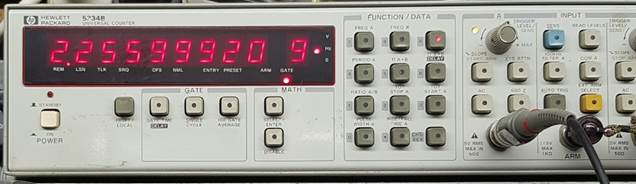
Figure 10 - Frequency with standalone TCXO within a few hundred Hertz at 2.256 GHz.
The output level etc. is shown in Figure 11. The -13dBm shown actually corresponds to the required +7dBm because I have a 20dB attenuator in the line to protect the Spec. An. ( -20 +7 = -13dBm). We can also see the second harmonic at around 4.5GHz is over 30dB down, primarily due to being within the native VCO range, and the natural LPF behaviour of the amp.
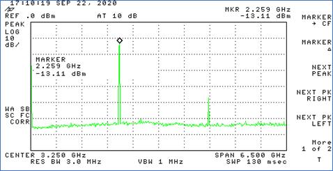
Figure 11 - With 20dB attenuator in line ie. -13 = +7 dBm.
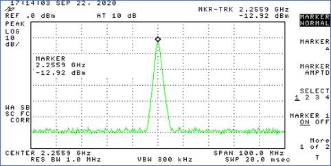
Figure 12 - Up close looking reasonably clean.
Figure 12 shows the same thing but zoomed in on the main signal which is looking nice and clean.
As a final word though don’t forget the ADF4350 output (particularly) for frequencies below about 2.2GHz is a square wave, and thus will have quite high harmonics. Figure 13 shows the output when set for 1150MHz, the required LO for a 23cM (1296MHz) transverter with 2m IF. In many cases the fact that the second and third harmonics are only 10-20dB down will not be an issue due to filtering in the Transverter, but in some cases it will make a real mess, so have a care.
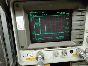
Figure 13 - While the LO will work down to 138MHz it is a square wave so watch out for harmonics.
73 Paul VK3DIP.
Back
Home