By Paul McMahon VK3DIP
Back
Home
As appeared in NERG NEWS February/March/May 2021
Source Etc.
PC Board Artwork in Sprint Layout Format
NEW !!!!!
Latest Part 4 using rotary encoder.
Part 1. Background and Design
Continuing with the idea of rebuilding my 2.4GHz transverter, I wanted a very stable 10MHz source to drive the Local oscillator PLL. The simplest stable signal source to build these days is one tied to the Global Positioning System (GPS). For the GPS to work it needs very stable timing and precise frequencies and so the base infrastructure uses a whole heap of atomic clocks etc. By locking/synchronizing an oscillator to GPS you can end up with something as accurate as those primary standards that are used to drive the GPS. When you do this it is called a GPS Disciplined Oscillator, or GPSDO.
There are many examples of GPSDO’s out there but they pretty much all use the same principle of locking via some form of a Phase or Frequency Locked Loop (PLL, or FLL) the oscillator in a GPS receiver (which is already locked to those very accurate standard sources via the GPS satellites) to another oscillator at the standard frequency desired.
The hard bit in this is getting a GPS receiver that lets you get at that core oscillator. Almost all GPS receivers offer a very accurate one Pulse Per Second (PPS) output tied to the locked internal oscillator, and there are a number of GPSDO designs out there that use this one PPS output. The difficulty with this is that one second between updates makes for a very cumbersome control loop. A GPS receiver with a higher frequency PPS output makes for a much simpler PLL structure.
There are a number of designs out there that utilize a somewhat older Trimble GPS receiver module, that you used to be able to get cheaply on the surplus/ebay/Aliexpress market, that had a 10kHz output as well as the 1 Hz PPS locked to the internal receiver master oscillator. Two typical examples of this can be found at the below web sites.
http://www.jrmiller.demon.co.uk/projects/ministd/frqstd0.htm
http://www.ntms.org/files/n1jez_ntms.pdf
Finding those Trimble modules has got pretty hard, but luckily there is a simpler cheaper option that is currently widely available at very low prices via ebay/Aliexpress, the u-Blox modules. You will find these on those sites as small GPS receiver modules typically targeted at Model Plane, Boat etc. enthusiasts, to provide on board navigation/tracking systems. The ones I am interested in here utilize the u-Blox NEO 7 component. According to the data sheet these components can be programmed to produce a PPS output ( u-Blox calls this the TimePulse output) locked to the internal 48MHz master oscillator anywhere between 0.25Hz and 10MHz, the default for this is 1 Hz. In practice many people have reported being able to produce other frequencies all the way up to the 48MHz master value, but I wouldn’t want to rely on this out of spec. performance. u-Blox produces a large number of GPS receiver modules some of which are listed along with their data sheet claims in Table 1 below.
|
GPS Module |
Possible TimePulse Frequencies |
|
AMY-6 |
? |
|
UC-530 |
1Hz |
|
UP-501 |
1Hz |
|
IT-530 |
1Hz |
|
LEA-5 |
0.25Hz-999Hz |
|
LEA-6 |
0.25Hz-1kHz |
|
LEA-6T |
0.25Hz-10MHz |
|
LEA-7 |
0.25Hz-1kHz |
|
LEA-M8F |
0.25Hz-2Hz |
|
LEA-M8S |
0.25Hz-10MHz |
|
MAX-M5Q |
1Hz |
|
MAX-6 |
0.25Hz-1kHz |
|
MAX-7 |
0.25Hz-1kHz |
|
MAX-M8 |
0.25Hz-10MHz |
|
NEO-6G/Q/M/P/V |
0.25Hz-1kHz |
|
NEO-6T |
0.25Hz-10MHz |
|
NEO-7M |
0.25Hz-10MHz |
|
NEO-7N |
0.25Hz-10MHz |
|
NEO-7P |
0.25Hz-10MHz |
|
NEO-M8 |
0.25Hz-10MHz |
|
PAM-7Q |
0.25Hz-1kHz |
|
CAM-M8Q |
0.25Hz-10MHz |
|
EVA-7M |
0.25Hz-10MHz |
Table 1 - uBlox GPS receiver Modules TimePulse capabilities
There are lots of Neo-6M’s out there but be careful, they are only rated to be able to produce a TimePulse at up to 1KHz. If that is what you want then OK, but in my case I wanted a higher reference 100KHz, so the Neo-7 or greater is the way to go. As far as the sub model ( the G,M,P,N,T etc.) is concerned the 6T would be a good one (the T stands for Timing and this is the one u-Blox themselves recommend for GPS timing applications like a GPSDO,) the T models have a Temperature Controlled crystal Oscillator master (TCXO). The M models are what you will find most often as they are the cheapest ones as they have only a standard ie. non temperature compensated crystal oscillator, and as will be discussed later they don’t have any included flash/non-volatile memory to store configuration details (such as TimePulse value) between one session and the next. Some examples of the various modules you will find on these sites, and the core u-Blox bit, are shown below in Figure 1, and Figure 2. There is some mention on various web sites about “fake” u-Blox modules, but I have bought a few and have not had any problems so far. As you can see there are several variations most obviously around the GPS antenna arrangement, but also less obviously as to the computer interface, the two most common being a four, and a five pin interface. The fifth pin is the PPS output so this is the most desirable one for a GPSDO, you can use a four pin one but this requires some fiddly on board mods.
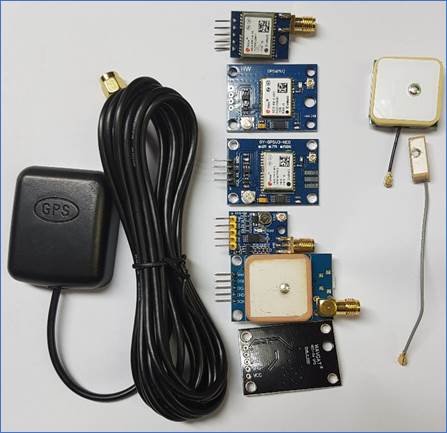
Figure 1- Example uBlox based GPS receiver modules and some GPS antennas.
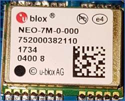
Figure 2- the uBlox Neo-7M component.
So you may ask why do I need anything else , why not just tell the Neo-7 to produce a 10MHz TimePulse and you are done? Well you can, but the master internal oscillator frequency is 48MHz, and to get 10MHz from 48MHz you need to divide by 4.8, ie. a non-integer number. This can and is done inside the u-Blox block but fractional division requires some tricks that lead to an effective or average division by 4.8 which leads to jitter and noise etc. which is undesirable in a frequency reference. So the answer is to pick a TimePulse that is an integer sub multiple of 48MHz , and then lock using that as a reference and a simple PLL to an external oscillator at the required frequency. There is another reason you want to do this, in that the cheaper M models only have a standard oscillator and while they will on average be very accurately locked to the GPS references they will as they drift require internal tweaking etc. from the u-Blox internal PLL, which in itself will create noise etc. By using a PLL to lock an external oscillator you can inherit some of the characteristics of that external oscillator, which can be considerably better than the M internal one. So in my case I picked 100KHz which is an integer sub multiple of 48MHz which also happens to be an integer sub multiple of 10MHz to make the PLL divider simpler. You could also use 2MHz or 1 MHz but I wanted to minimise internal radiation, and impedance matching problems, that would have occurred as the cheap modules don’t provide a coaxial output for the PPS.
The circuit diagram for the core PLL is shown in Figure 3. As you can see the choice of 100KHz for the reference means only three 14 pin High Speed CMOS (HCMOS) digital integrated circuits are required , a 74HC86 quad Exclusive OR, a 74HC390 dual decade divider, and a 74HC14 hex Schmitt trigger input invertor. HC logic comfortably handles the 10MHz max seen here.
As shown in the diagram several components are marked with asterixis, these components may not be needed in all cases or could need to be different values. These all vary primarily due to what is used as the locked oscillator. The loop filter components are affected by the gradient of the oscillator, its variable oscillator gain in variation of frequency (Hz) out per variation of control voltage (V) in. The AC coupling of the oscillator output, and mid-point bias of the following invertor is required if the oscillator has a non 5v digital level output.
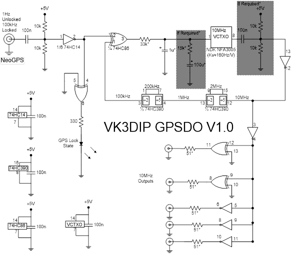
Figure 3- Core GPSDO PLL
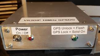
One of the other nice features of the u-Blox GPS receiver modules is that the TimePulse can be programmed to be different depending on the status of the GPS receivers own lock state. In my case I program them to be 1Hz (50% duty cycle) unlocked, and 100KHz (50% duty cycle) locked. As well as using this as the reference for the PLL, I also bring this to a LED on the front panel to indicate GPS lock status, the 1Hz is obviously flashing, the 100KHz looks like an always on. The 50% duty cycle is required to have the simple XOR phase detector work correctly.
The other variable in this circuit is how many and of what type outputs are required. As shown above with 51 Ohm resistors it has five separate, relatively low power outputs. If higher powered outputs are required, then the gate outputs can just be paralleled up as shown in Figure 4. If two outputs are paralleled then the two resistors should be 100 Ohms, if three 150 Ohms, four 200 Ohms and so on. As well as having higher powered digital outputs, it is also possible to AC couple and add a 10 MHz lowpass filter to produce a reasonably clean sinewave output. Note, while the resistor values mentioned will nominally match the outputs to 50 Ohms, if you intend to use multiple outputs be aware that just connecting up to 50 Ohm loads may pull more than the safe recommended output from each gate. More on this later.
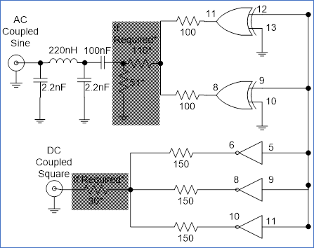
Figure 4 - Output options.
The simplest way to configure these GPS receiver modules is using the uBlox U-Center software which can be downloaded from here: https://www.u-blox.com/en/product/u-center . The PC is connected to the module, usually via a USB to serial convertor with the default speed of 9600 baud. The relevant section of U-Center for TimePulse configuration is shown in Figure 5.
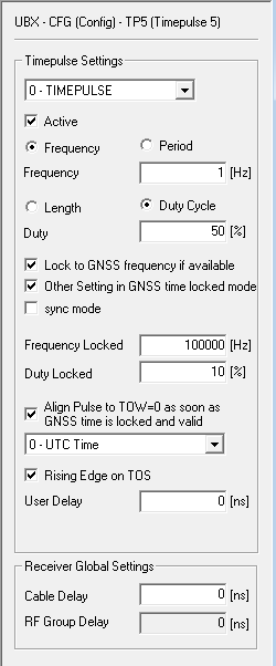
Figure 5 - U-Center showing TimePulse Configuration
Unfortunately, just setting the TimePulse to something other than the 1Hz default via U-Center is not the end of it. The cheapest and most readily available “M” modules don’t have non-volatile memory in the Neo-7 itself, the usually provided onboard backup supercap will maintain settings for some hours of powered down but not much longer. The small modules do also usually have a separate flash memory chip outside the Neo-7, however at least in the ones I have tried the TimePulse setting is not one of the things saved/auto recovered on startup. So, you need something to effectively program the GPS module every time it is powered up. In my case I used an Arduino Nano to do this as per Figure 6
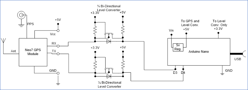
Figure 6- Adding a microcontroller to program the GPS.
Note the need for the 5v to 3.3v logic level convertors to go between the Nano running at 5v and the GPS receiver running at 3.3v (even though the module Vcc in is 5v, that just powers an on board 3.3v regulator). These level convertors come four on a small board for less than a dollar from the usual sites. The code (Arduino INO file) I use is shown in the appendix, along with a sample output. So in that code what I do is set the TimePulse to 100KHz, and the receiver mode to Stationary, and keep doing that until the module acknowledges successful setting of both. Stationary mode is the best mode for timing applications as it assumes that the antenna is not moving, which enables the receiver to maintain a timing lock even if it gets down to only a small number of satellites being visible. Once I get successful setting I cut through to a mode where the Nano is effectively just being used as a bidirectional USB to serial convertor. Ie. the USB output from the nano will contain the normal GPS receiver text stream that may be useful to look at with U-Center , or if your contesting program say could use it to pick up the UTC time etc. To work out what values etc. to send to the GPS module to achieve the settings I wanted I captured the binary stream between U-Center and the module using its built-in capture functions. I also looked in the data sheets, but a cut and paste from the capture saved some typing and calculation of checksums etc.
The final part of the circuit is the voltage regulators as shown in Figure 7. If you have an oscillator that doesn’t draw too much current at 5V you can get away with no heatsink on the 7805, this can be helped further by sharing the power dissipation by including a 7808 8V pre regulator as shown. If you have an oscillator that draws several hundred milliamps at startup then you really need to have the 7805 either bolted to a solid metal case or suitable heatsink.
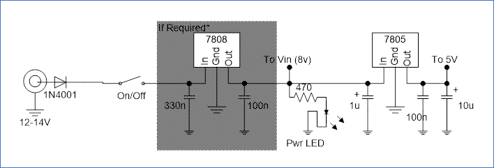
Figure 7 Voltage Regulators
In the next part I will give more details of building the GPSDO and how to allow for different 10MHz oscillators.
73 Paul VK3DIP.
Part 1 Appendix , Arduino Code and Example Start up run output.
/*
GPSDO setup TP5 and communicate
VK3DIP V1.0 25/08/2020
Initial Version Set TP and Cut Through
VK3DIP V1.1 20/10/2020
Add set Nav Mode to Stationary to optimise TP stability.
Based on code found at https://ukhas.org.uk/guides:ublox6
Additional Code by J Coxon (http://ukhas.org.uk/guides:falcom_fsa03)
*/
#include <SoftwareSerial.h>
SoftwareSerial GPS(4, 3);
byte gps_set_sucess = 0 ;
void setup()
{
// Start GPS Serial at default 9600
GPS.begin(9600);
// Start USB/Serial back to PC also 9600
Serial.begin(9600);
Serial.println(" ");
Serial.println("Neo-7+ GPSDO ");
Serial.println("VK3DIP V1.1 Oct. 2020");
Serial.println("Initialize TP to 100KHz ...");
// This UBX command sets the TimePulse to 1HZ unlocked, 100KHz Locked, both 50% duty cycle
Serial.println("Setting uBlox TP5 mode: ");
uint8_t setTP5[] = {
0xB5, 0x62, 0x06, 0x31, 0x20, 0x00, 0x00, 0x01, 0x00, 0x00, 0x32, 0x00, 0x00, 0x00, 0x01, 0x00,
0x00, 0x00, 0xA0, 0x86, 0x01, 0x00, 0x00, 0x00, 0x00, 0x80, 0x00, 0x00, 0x00, 0x80, 0x00, 0x00,
0x00, 0x00, 0xEF, 0x00, 0x00, 0x00, 0xA1, 0xBA };
while(!gps_set_sucess)
{
sendUBX(setTP5, sizeof(setTP5)/sizeof(uint8_t));
gps_set_sucess=getUBX_ACK(setTP5);
}
gps_set_sucess=0;
Serial.println("TP Set successfully ");
// This UBX command sets the Navigation Mode to Stationary which is optimal for accuracy of Time Pulse
Serial.println("Setting uBlox Nav mode: ");
uint8_t setNav[] = {
0xB5, 0x62, 0x06, 0x24, 0x24, 0x00, 0xFF, 0xFF, 0x02, 0x03, 0x00, 0x00, 0x00, 0x00, 0x10, 0x27,
0x00, 0x00, 0x05, 0x00, 0xFA, 0x00, 0xFA, 0x00, 0x64, 0x00, 0x2C, 0x01, 0x00, 0x3C, 0x00, 0x00,
0x00, 0x00, 0x00, 0x00, 0x00, 0x00, 0x00, 0x00, 0x00, 0x00, 0x4E, 0x60 };
while(!gps_set_sucess)
{
sendUBX(setNav, sizeof(setNav)/sizeof(uint8_t));
gps_set_sucess=getUBX_ACK(setNav);
}
gps_set_sucess=0;
Serial.println("Done now cutthrough ...");
Serial.println(" ");
}
void loop()
{
while(1)
{
if(GPS.available())
{
// Read GPS Serial inputs (if available) and send them to the USB/Serial/PC
Serial.write(GPS.read());
}
//Read USB/Serial/PC inputs (if available) and send them to GPS module
if(Serial.available()){
GPS.write(Serial.read());
}
}
}
// Subs and functions
// Send a byte array of UBX protocol to the GPS
void sendUBX(uint8_t *MSG, uint8_t len) {
// Serial.println("Send UBX Command:");
for(int i=0; i<len; i++) {
GPS.write(MSG[i]);
if ( i % 10 == 0 && i != 0) Serial.println() ;
PrnHEX(MSG[i]);
}
GPS.println();
}
// Print Hex Chars nicely.
void PrnHEX(uint8_t MyChr) {
Serial.print("0x");
Serial.print(MyChr < 16 ? "0" : "");
Serial.print(MyChr, HEX);
Serial.print(" ");
}
// Calculate expected UBX ACK packet and parse UBX response from GPS
boolean getUBX_ACK(uint8_t *MSG) {
uint8_t b;
uint8_t ackByteID = 0;
uint8_t ackPacket[10];
unsigned long startTime = millis();
Serial.println();
Serial.print("Reading ACK response: ");
Serial.println();
// Construct the expected ACK packet
ackPacket[0] = 0xB5; // header
ackPacket[1] = 0x62; // header
ackPacket[2] = 0x05; // class
ackPacket[3] = 0x01; // id
ackPacket[4] = 0x02; // length
ackPacket[5] = 0x00;
ackPacket[6] = MSG[2]; // ACK class
ackPacket[7] = MSG[3]; // ACK id
ackPacket[8] = 0; // CK_A
ackPacket[9] = 0; // CK_B
// Calculate the checksums
for (uint8_t i=2; i<8; i++) {
ackPacket[8] = ackPacket[8] + ackPacket[i];
ackPacket[9] = ackPacket[9] + ackPacket[8];
}
while (1) {
// Test for success
if (ackByteID > 9) {
// All packets in order!
Serial.println(" (SUCCESS!)");
return true;
}
// Timeout if no valid response in 3 seconds
if (millis()-startTime > 3000) {
Serial.println(" (FAILED!) Try Again");
return false;
}
// Make sure data is available to read
if (GPS.available()) {
b = GPS.read();
// Check that bytes arrive in sequence as per expected ACK packet
if (b == ackPacket[ackByteID]) {
ackByteID++;
PrnHEX(b);
}
else {
ackByteID = 0; // Reset and look again, invalid order
}
}
}
}
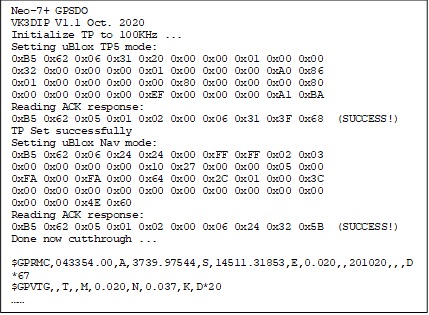 Example
output from Arduino Nano on start-up as seen in Serial Monitor in Arduino IDE.
Example
output from Arduino Nano on start-up as seen in Serial Monitor in Arduino IDE.
Part 2. Building it.
After the GPS module the locked oscillator is probably the most important part of the GPSDO. The quality and performance of this oscillator will directly affect/contribute to the performance of the GPSDO. Basically the better the oscillator the better the GPSDO.
So, what do you need and where do you get it?
There are several different possible oscillator types, the three most common from least good to best, are the Voltage Controlled Crystal Oscillator (VCXO), the Voltage Controlled Temperature Compensated Crystal Oscillator (VCTCXO) , and the Voltage Controlled Oven Controlled Crystal Oscillator (VCOCXO). Unfortunately in the case of the last two it is common to leave the VC part of the name off the description, so it needs a good look at a data sheet or equivalent to see if they actually are voltage controlled or not. Obviously if they are not voltage controlled you can’t lock them in the loop. You could also theoretically use a simple Voltage Controlled Oscillator (VCO) but this probably would be no better than what comes out of the GPS module itself. Crystal Oscillator output frequency is temperature sensitive, ie. as the temperature of the quartz varies its resonant frequency will also (slightly) vary. A VCXO has nothing to handle temperature variations other than the external loop itself, which it will do, however this constant variation can introduce small amounts of noise/jitter into the resultant output. A VCTCXO goes one better by including additional components in the oscillator itself to attempt to compensate for the effects of temperature change. This compensation is however not perfect so there may still be some loop variations as it tracks. The VCOCXO is the best case where the crystal oscillator is kept at a constant (usually high) temperature ie. Ovened, so there is no variation in frequency except at extreme temperatures.
Anyway, you could buy one of any of these new from one of the bigger electronics component sellers, but there are two problems with this. Firstly, pretty much all that are available new these days are made physically small and for surface mounting which can be a problem for Amateur construction. Secondly, and perhaps more importantly, they can be quite expensive, even a VCXO could be the single most expensive component in the GPSDO, and a good OCXO might be several tens of times the entire cost of the rest of the GPSDO! Fortunately, there are alternatives, you may be lucky as I was, in finding a suitable oscillator on an old PCB from something like a commercial transceiver, which is where the NDK TCXO shown below came from. Otherwise there seems to be at the moment quite a number of second-hand 10MHz OCXO’s on Ebay and AliExpress. Prices can be as low as $5 each in lots of 4. These OCXO’s seem to have been recovered from junked commercial equipment PCB’s, possibly mobile phone base stations, usually using some form of a saw, as they often come still soldered to a fragment of PCB. The problem with using a second-hand oscillator is that usually finding data on them can be problematic. In this case the fragment of PCB supplied can be useful in at least identifying the probable pinout. (see Figure 8 ) Once you have the pinout the other bits of info you need can be experimentally determined. Also the fact that the oscillator is used can be a positive as it is believed that crystal oscillators especially ovened ones can actually improve quality, stability, etc. with age. (like wine Greg :) )
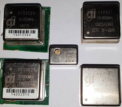
Figure 8 - Example oscillators
Given that you manage to find a second hand oscillator (and it works) the main things you need to figure out are:
1. Supply Voltage. You can probably figure this out by looking at the remnants of the PCB it came with, or if you are very lucky by finding some data for it on the internet. If still not sure the ground pin is usually obvious as being connected to the case, assume the most common pinout that has the same layout and ground in the same spot, and starting with 3.3V gradually increase the supply voltage until you get a clean output. Most of the old ones I have found are 5V, but some of the really good (large) ones are 12V or greater. By the nature of ovened oscillators they will get hot but hopefully not smoke.
2. Output type, Square or Sinusoid, Voltage levels, and AC or DC coupled. A CRO is the easiest way to find this. If AC coupled or the levels are less than say 4V, you need to install the optional series capacitor and pair of 10KΩ bias resistors. The actual square or sinusoidal nature of the wave form doesn’t matter that much as the Schmitt trigger inputs should square things up, and the final divider by two in the 74HC390 should guarantee 50% duty cycle to the phase detector. If the output level is over 5V pp then a suitable resistive voltage divider is required.
3. Voltage gain or Kv. This is the change in output frequency for the change in input frequency, it will usually be some Hz to hundreds of Hz per one volt voltage change on the control input. You don’t need a particularly accurate frequency meter for this just one that can show Hz at 10MHz, and the variable voltage source can be just say a 10K potentiometer from 5V to ground with the wiper going to the control input. In my case I plot the result in excel and use the trendline to give me the gradient as shown in Figure 9 and Figure 10 below. Alternately even just moving the control by a volt , preferably around the 10MHz mid point and noting the difference between the two frequencies would be good enough.
4. Measure the current required at start-up, and steady state. This is particularly important in the OCXO case as even the small ones can draw just under an Amp at start-up while the oven is heating, dropping down to a couple of hundred milliamps once up to temperature. You need to set the voltage regulator/s up with heatsinks etc. to accommodate this load.
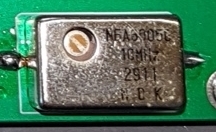
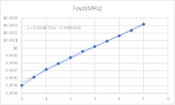
Figure 9 - NDK VCTCXO -157Hz/V
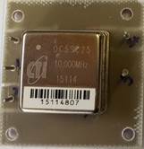
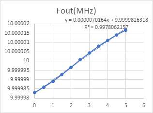
Figure 10- CTI OC5SC25 – 7Hz/V
Once you know the value of Kv you can work out the required values for the loop filter.
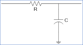
Figure 11 Simple RC Lag loop filter.
Calculating the values for a first order Lag RC loop filter
(Figure 11) is pretty simple. If we assume the EXOR phase detector, and with
the loop division of 100 as in the basic design (10MHz to 100KHz) and if we
also chose critical damping and a C value of 1uF then the R (in Mega-Ohms i.e.
MΩs) required is simply given by ![]() . Alternately if we use 10uF for C
then R (in KΩs) becomes
. Alternately if we use 10uF for C
then R (in KΩs) becomes ![]() . So for
example with my OC5SC25 with a Kv of 7Hz/V, with C of 10uF we get
. So for
example with my OC5SC25 with a Kv of 7Hz/V, with C of 10uF we get ![]() or 71.4KΩ, which I get
close to (71.33KΩ) by using 330KΩ in parallel with 91KΩ. I
could undoubtably have got away with using a single 75KΩ resistor, but I
didn’t happen to have one of that value on hand at the time. For the NDK TCXO
with Kv of 157 and 1uF we get 31.8KΩ for which I used a 33KΩ and
that worked fine. Obviously, different C values can be used but I had a few 1uF
and 10uF 16v Tantalums on hand and their lower losses make them ideal for this
application. We can get away with this sort of simple filter in this case as
the reference frequency is reasonably high, and unlike a PLL in a transceiver
etc. that needs to be able to lock to multiple frequencies we only have a
single frequency here with hopefully no modulation or step changes. I did allow
for more complex filters in the circuit shown previously and on various
versions of the PCB, so feel free to experiment but be aware the calculations
for higher order filters are quite a bit more complicated and there are a few
more parameters to worry about.
or 71.4KΩ, which I get
close to (71.33KΩ) by using 330KΩ in parallel with 91KΩ. I
could undoubtably have got away with using a single 75KΩ resistor, but I
didn’t happen to have one of that value on hand at the time. For the NDK TCXO
with Kv of 157 and 1uF we get 31.8KΩ for which I used a 33KΩ and
that worked fine. Obviously, different C values can be used but I had a few 1uF
and 10uF 16v Tantalums on hand and their lower losses make them ideal for this
application. We can get away with this sort of simple filter in this case as
the reference frequency is reasonably high, and unlike a PLL in a transceiver
etc. that needs to be able to lock to multiple frequencies we only have a
single frequency here with hopefully no modulation or step changes. I did allow
for more complex filters in the circuit shown previously and on various
versions of the PCB, so feel free to experiment but be aware the calculations
for higher order filters are quite a bit more complicated and there are a few
more parameters to worry about.
As you will see in both the versions I have built so far, as well as some common IC’s and resistors etc. which are readily available from Jaycar etc., I used the small Neo-7 GPS module (search for something like Neo-7m GPS mini module) not because I needed it small, but because as mentioned before it has the 5 pin interface including the PPS. I used an external antenna (search GPA antenna SMA), an Arduino Nano (either Atmega168 or Atmega328 are fine), as well as a small logic level convertor board (search Bidirectional Logic level Converter). The rest is basically the PCB, and hardware of screws, sockets, etc. and some sort of box to put it in. In one version I repurposed a box got from a hamfest, and in the other I used a Jaycar HB5046 diecast box. I have so far produced 2 PCB’s for the GPSDO, the first V1.0 was a classic first version, it needs a small number of tweaks to work including one track cut and a jumper, but that is the version I used for both of the instances here. The V1.1 (Figure 14) is a slightly improved version with the main difference being I managed to squeeze in room for a 25mm square OCXO. In both cases the board can be separated into two if you want the loop separated from the GPS (see Figure 12) or used as one large board ( see Figure 13).
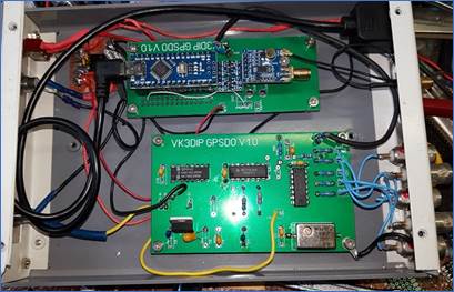
Figure 12 NDK VCTCXO version, separated boards in a repurposed case.
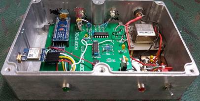
Figure 13 - OCXO version in a Jaycar HB5046 box.
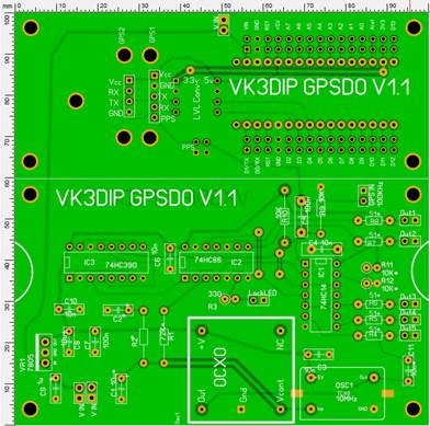
Figure 14 - Version 1.1 Board with provision for OCXO
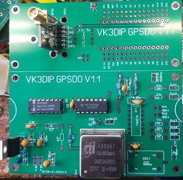
Figure 15 - Version 1.1 PCB under construction.
Apart from getting parts and working out the loop values, you also need to decide how you are going to configure the outputs. As mentioned before just putting in the series resistor to match to 50 Ohms and perhaps paralleling some outputs up may not be enough. One of the key factors is what do you want to drive. Examples of this are given in Table 2
Table 2. 10MHz Reference Requirements
|
Device |
Native Input Impedance |
Power requirement |
|
HP8590E Spec. An. |
50Ω |
-2dBm to +10dBm |
|
ZVB20 VNA |
50 Ω |
-5dBm to +10dBm |
|
HP5334B freq. Meter |
1KΩ//<20pF |
500mV to 5V |
|
IC-9700 |
50Ω |
-10dBm to 0dBm |
|
ADF4350 |
100KΩ |
logic levels |
As you can see there is a lot of differences and while most don’t care if it is a square or sine waveshape some do. If you intend to have the GPSDO some distance from the thing that requires the reference then the impedance matters, 50Ω is good for coax distribution, whereas high impedances like the 100k cause coax problems, the levels and power output requirements are also affected. If you just want to drive 5 or less ADF4350’s and they are not located at a distance then you can basically just use single outputs with the 51Ω series resistors. This will match the input end of the coax and not excessively load the gates, the output end of the coax going into 100KΩ is far from matched however and there will be reflections etc. which may be a problem. You can’t however just parallel up another 50Ω resistor at the end of the coax to improve the match, or for that matter just connect up to a 50Ω input, as this may result in over loading the gate’s output’s power handling capacity. With the prototypes I measured the following powers ( Table 3).
Table 3 Matched Power Outputs
|
Number of gates |
Type |
dBm (into 50Ω) |
Effective Per Gate Current (mA rms) |
|
1 |
HC14 |
8.7 |
12.2 |
|
1 |
HC86 |
10.3 |
14.6 |
|
2 |
HC86 (through filter) |
12.4 |
9.3 |
|
3 |
HC14 |
11.5 |
5.5 |
TI design guidelines and data sheets have the typical absolute maximum current for a HC gate at 25mA, but in practice recommend no more than 5.2mA per gate. So in these measurements all of these cases are over the 5.2mA, though the 3 HC14’s is pretty close and probably OK. In the other cases it would not be recommended to do this long term, especially with multiple simultaneous loads. Also paralleling different types of gates would probably not be a good idea as the different properties of HC86 and HC14 gates could lead to uneven current sharing and potentially crossover issues due to the different rise times/propagation delays. So the options here are to have up to 3 parallel HC14’s and up to 2 parallel HC86’s.
Also it should be noted you cannot use 50 Ohm attenuators by themselves to get the output levels down as they are still a 50 Ohm load and thus they do not decrease the gate dissipation. Pretty much the only way to get down to safe levels (where you can then use 50 Ohm attenuators if needed) is to compromise the impedance match somewhat by using additional series R. This can be just the series R by itself, or alternately series R followed by a shunt R as in an L pad. Because this can depend on the individual IC’s the simplest way is figure out what you need in terms of drive and then experimentally determine appropriate additional resistors. In my case for example an additional 30 Ohm resistor in series with the three HC14 gates in parallel got me within 0.1dB of 10dBm out into 50 Ohms and the currents down under the 5.2mA per gate. Likewise for the 2 HC86 case an L pad of a series 110 Ohms and shunt 51 Ohms got me pretty much exactly 0dBm out into 50 Ohms and in this case well under the 5mA per gate, in both cases the line match was slightly compromised but still close enough that line radiation etc. would not be a problem. These variations will probably come out as reasonably repeatable so if you just want to use the same values as I did then that may be simpler than playing with values, which is why I showed them in the earlier Figure 4.
I have made a few of these now and all have more or less worked with minimal problems straight away.
A few words and pictures on accuracy and stability. Figure 16, and Figure 17 show the spectrum of a TCXO and OCXO version respectively, the +/- 100KHz bumps from the loop frequency are noticeable but in both cases better than 60dB down on the fundamental. The OCXO one is slightly better ( note that the horizontal scale is different in the two cases.)
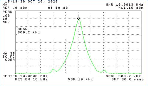
Figure 16 NDK Version in close.
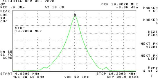
Figure 17 - OCXO version Square wave up close.
Looking at a wider frequency range it is easy to see the harmonics in the square wave case, ( Figure 18,) but they are considerably attenuated by even the single stage PI filter shown previously for a sinewave output (Figure 19).
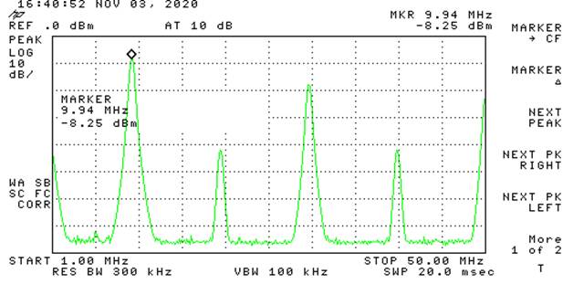
Figure 18 - OCXO square wave showing harmonics.
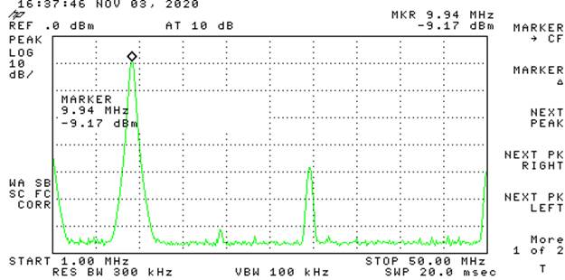
Figure 19 - OCXO Sinewave version filter significantly reducing harmonics.
Finally accuracy and stability, to the limits of my test equipment these GPSDO’s produce basically identical outputs to a commercial GPSDO. For example measuring the output frequency on a frequency counter locked to the commercial GPSDO (Figure 20), we get a value that is better than within 0.1 Hz of the desired output.
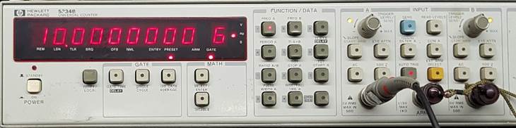
Figure 20 - Final result, output stable and accurate to better than 0.1 Hz.
In fact just measuring the Commercial GPSDO’s output and my GPSDO’s output on the same frequency meter shows that averaged over 100 gate intervals there is less than 0.01Hz difference between the two.
Part 3. Mods and Add Ons.
I made a Boo Boo.
First thing is the PCB, it usually takes, at least me, two or three shots to get it perfect, which is why the board houses offer a prototyping service I suppose. Anyway, on PCB board V1.1, if you happened to have got one from the NERG, there is one fairly major problem (Vin is shorted to earth!) luckily it is very easily corrected. I will fix it in the V1.2 version, but in the meantime the relevant area is on the back of the board behind the two Vin connector pads that are next to each other, I missed a track clearance which has ended up shorting these connectors out. The fix is simple, find the area affected, see closeup Figure 1, and two small cuts with a Jiffy or Stanley knife and it is all fixed. Be sure to verify this with a multi-meter test before applying power. If you don’t the results will be pretty obvious!
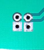
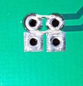
Figure 1 Oops that’s a short before and after.
A Resistive Splitter.
The first add-on I made was a resistive three-way (one in three out) splitter for the 10MHz output. With the three outputs of the 74HC14 paralleled/terminated as described last time I typically get 10 to 11 dBm out, with the roughly 9.5dB loss of the splitter that gives me about, or just over, +1dBm out of each of the three ports. I have found 1dBm to be a convenient level as it satisfies the IC9700, the terminated reference in of the ADF4350 that I use for my transverters, and most of my other test equipment. I made the splitter on a scrap of PCB with some board mount BNC’s bought cheap from Rockby some time back, and another thin strip of PCB glued on the back to form the common land. I also used 27Ω resistors rather than the nominally exact 25Ω because 27 is a common/standard value which I had, and it is within 10% of 25 so I don’t expect problems especially at 10MHz. See Figure 2 for details.
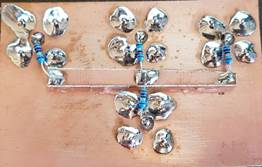
Figure 2 Front and back of splitter.
An LCD Display.
The next add-on requires some code changes in the Arduino Nano to drive it, as shown in the initial photo above, it is a small LCD display. The display used is the commonly available 2 line 16 character LCD display which I have used via a special I2C interface. The displays are available for $3-4 from the usual online merchants as are the I2C interface boards (typically $1.50). Sometimes you can get the two already connected in a single purchase to save yourself a bit of soldering. The advantage of this sort of display is you only need to connect up four wires from the interface board to the GPSDO board; +5v, Earth, and the SDA (data), and SCL (clock) lines. I brought out all the IO lines from the Nano onto the GPSDO board so this is a very easy connection. The +5 can come from the +5 out of the Nano, which is good as it means the display will work when you plug a USB line in between your PC and the unit to program it. But it also is not capable of delivering too much power, so if you go for a big display with a hungry backlight, it is better to connect to one of the 5v lines on the logic /oscillator part of the board which can deliver more power. The earth can go to any convenient ground point such as on the NANO breakout, and the SDA and SCL wires go to the outputs marked as A4 for the SDA and A5 for the SCL as shown in Figure 3.
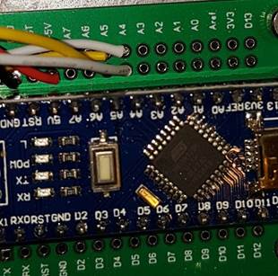
Figure 3 - I2C lines A4=SDA, A5=SCL
Figure 4 shows the I2C display controller mounted on the back of the LCD module. You can see the four connections back to the GPSDO board going in my case via what is called a dupont connector . These connectors are available for however many pins you require if you want to make them up yourself, but I being lazy, prefer to buy either single/double ended pigtails/cables already made up from the usual online sources. You can also see the trim pot that is for adjusting the display contrast.
The most important thing to note however is that these modules can come with a PCF8574 chip from one of several different manufacturers and they are not exactly the same! I2C communications relies on knowing the correct address for the peripheral device, and probably just to be difficult some of the chip foundries chose different default addresses for their PCF8574 chips.
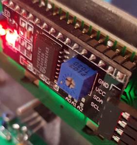
Figure 4- I2C display controller mounted on back of LCD.
You can also see the A0-A2 address set solder jumpers under the contrast trimmer, but even using these you can’t set the different chips to use the same address. I have been caught by this before, in most of the interfaces I have got recently, the default interface address has been 0x27 (or 39 decimal) so that is what I use in my code, but 0x3F (63 decimal) is not unknown! So if your one doesn’t work (after adjusting the contrast of course) you may need to alter the code. The relevant line is:
LiquidCrystal_I2C lcd(0x27,16,2);
Just make the 0x27 into 0x3F and recompile/load and see how you go.
For my display as well as various startup and diagnostic messages I chose to display the items shown in Figure 5.
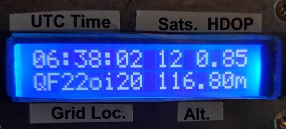
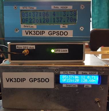
Figure 5 - My Display.
I chose these items both, because they would be useful, and because I could satisfy them from a single NEMA message (GGA) from the Ublox GPS. I could then turn off all the other messages and considerably improve the responsiveness of the Nano’s processing. The UTC time and 8 character Grid locator (my home QTH in this case) should be familiar to most hams, they are provided directly by the GPS and calculated from the Lat and Long, the Altitude is probably equally obvious again coming directly from the GGA message, leaving only the number of satellites used and Horizontal Dilution Of Precision (HDOP) to explain. Basically, the number of satellites and HDOP give an indication of how good a fix the GPS is currently providing. The more satellites the better (max for the neo7/8 is 12), and the smaller the HDOP the better, just less than one (as shown) is probably as good as you will get with a 12 channel GPS, 100 is “I have no idea”. Luckily for GPSDO purposes we don’t need that good a fix to accurately “discipline” the oscillator, but I wouldn’t trust it if the number of satellites was less than say 3, or HDOP was over say 10.
I want something other than 10MHz out.
While the most common external reference frequency used is 10MHz, in some cases it is nice to have other frequencies also GPS disciplined. For example in my case while the 10MHz locks my 2.4GHz transverter, the FT817 I use for the IF only has a TCXO, and a cheap clone one at that. In the FT817 case the TCXO master oscillator runs at 22.625MHz, which is not easily obtained from 10MHz unless you use some sort of PLL arrangement. Enter the SI5351 board. This board, yet again available from the usual online sources for <$10, is shown in Figure 6.
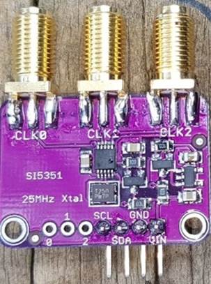
Figure 6- SI5351 Board
This little board can produce three independent (square wave) clock outputs anywhere from 10’s of KHz to 100’s of MHz and only requires a standard I2C connection (as in the display case above) to drive it. You will note however it uses an on board 25MHz crystal as a reference, which is only slightly less difficult to produce from 10MHz, also the data sheet says only 25MHz to 27MHz is possible for the crystal. Two things however, there is a more expensive variant of the chip that comes with an external reference in pin, which the data sheet lists as being 10MHz to 100MHz capable so most Arduino code libraries allow this range for reference, plus the data sheet also says you can drive the XA oscillator pin directly via a 100nF capacitor. Putting these two facts together, can we make an external reference in equivalent on the cheap readily available board? A bit of googling found http://www.simonsdialogs.com/2018/11/si5351a-any-frequency-cmos-clock-generator-and-vco-specifications-myths-and-truth/ and yes it appears you can.
So basically, you carefully remove the 25MHz crystal (hot air tool etc.) see Figure 7. This also shows which pad you need to connect the external reference into.
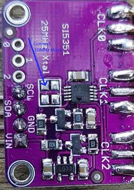
Figure 7 - Remove Crystal
Then I used a SMD 100nF capacitor , but you could use a small leaded 100nF ceramic if that is what you had, to connect via a short length of hookup coax back to an unused 10MHz output back on the GPSDO board. In my case I used one of the 74HC86 outputs leaving the 51Ω series resistor in circuit for a bit of current limiting, and it worked a treat. See Figure 8
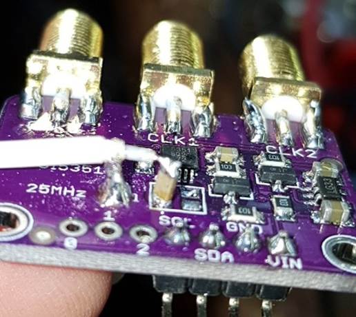
Figure 8- connection to external 10MHz Ref
By driving the SI5351 from the disciplined 10MHz any output from the SI5351 should be just as accurate as the 10MHz itself.
In my code I picked as well as the 22.625MHz two other frequencies from a quick google of common Ham reference frequencies. The relevant lines of code are:
// Set CLK0 to output 22.625 MHz for Yaesu FT8x7
si5351.set_freq(2262500000ULL, SI5351_CLK0);
// Set CLK1 to output 15.6 MHz
si5351.set_freq(1560000000ULL, SI5351_CLK1);
// Set CLK2 to output 30.2 MHz
si5351.set_freq(3020000000ULL, SI5351_CLK2);
Edit them to suit your requirements but note if you want >100MHz you may have to use a bit more code to set which of the internal PLLs is used etc. see the SI5351 arduino library docs for more info.
Yes it works well. See Figure 9.
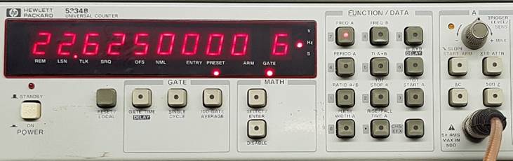
Figure 9 Clk 0 out after GPS lock.
Connection of the SI5351 module is just as simple as the display, it happily shares the same I2C SDA SCL lines from the Nano as it has a different address (0x60 or 96 in decimal), than either of the display variants.
The complete expanded GPSDO internals is shown in Figure 10 , note the use of connectors to make connection to the various modules easy. The display is to the bottom right (front wall) in the figure, the Neo (in this case 8) GPS module is on the left side wall, and the SI5351 board is on the top (back) wall. Also note that the interconnect coax for the reference of the SI5351 is passed though one of the unused mounting holes on the SI5351 board to help prevent stress fractures of the SMD capacitor soldered on its end to the board. The missing components on the main board are optional and or not required for this particular OCXO . For example the display negates the need for power or lock leds, so I didn’t use them here.
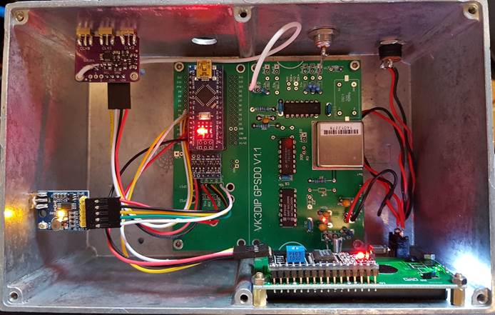
Figure 10 -Inside of GPSDO with add on’s
Conclusions
This GPSDO has proved to work quite well, or at least at the recent John Moyle contest no-one complained I was off frequency, or had birdies etc. hi-hi. It is a reasonably inexpensive way of never having to have that “who is not on the correct frequency” discussion ever again. I have placed a zip of the original and upgraded source (ino) files here: http://www.yagicad.com/VK3DIPGPSDOSRC.zip if anyone wants them. The code is very simple and forgiving, for example if you don’t install the display or the SI5351 board it will still all work and only make note of it back via the USB (if connected) to a serial monitor on the PC. Have a go it really isn’t that hard to make it work.
73 Paul VK3DIP.
Back
Home